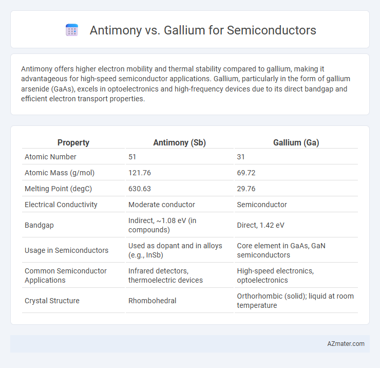
Antimony offers higher electron mobility and thermal stability compared to gallium, making it advantageous for high-speed semiconductor applications. Gallium, particularly in the form of gallium arsenide (GaAs), excels in optoelectronics and high-frequency devices due to its direct bandgap and efficient electron transport properties.
Table of Comparison
| Property | Antimony (Sb) | Gallium (Ga) |
|---|---|---|
| Atomic Number | 51 | 31 |
| Atomic Mass (g/mol) | 121.76 | 69.72 |
| Melting Point (degC) | 630.63 | 29.76 |
| Electrical Conductivity | Moderate conductor | Semiconductor |
| Bandgap | Indirect, ~1.08 eV (in compounds) | Direct, 1.42 eV |
| Usage in Semiconductors | Used as dopant and in alloys (e.g., InSb) | Core element in GaAs, GaN semiconductors |
| Common Semiconductor Applications | Infrared detectors, thermoelectric devices | High-speed electronics, optoelectronics |
| Crystal Structure | Rhombohedral | Orthorhombic (solid); liquid at room temperature |
Introduction to Antimony and Gallium in Semiconductors
Antimony (Sb) and Gallium (Ga) serve distinct roles in semiconductor technology, with Antimony often used as a dopant element to enhance n-type conductivity in materials like silicon and gallium arsenide (GaAs). Gallium is a fundamental component of compound semiconductors such as GaAs and gallium nitride (GaN), critical for high-speed electronics and optoelectronic devices due to their superior electron mobility and direct bandgap properties. The combination of Antimony and Gallium in semiconductor alloys enables tailoring of bandgap and electrical properties for applications in infrared detectors, lasers, and high-frequency transistors.
Chemical and Physical Properties Comparison
Antimony exhibits a higher atomic number (51) and density (6.697 g/cm3) compared to gallium, which has an atomic number of 31 and a density of 5.91 g/cm3, influencing their distinct semiconductor applications. Gallium has a melting point of about 29.76degC, making it a low-melting metal, whereas antimony's melting point is significantly higher at 630.63degC, contributing to different thermal stability in devices. Chemically, gallium forms stable compounds like gallium arsenide (GaAs) widely used in high-speed electronics and optoelectronics, while antimony is primarily used as a dopant in semiconductor alloys and compounds like lead antimonide for thermoelectric applications.
Electrical Conductivity and Bandgap Analysis
Antimony exhibits higher electrical conductivity than gallium due to its lower resistivity and more metallic bonding characteristics, making it favorable for certain semiconductor applications requiring efficient charge transport. Gallium, particularly in compounds like gallium arsenide (GaAs), offers a wider bandgap (~1.42 eV) compared to antimony-based semiconductors, leading to superior electron mobility and high-frequency performance. Bandgap analysis indicates gallium's advantage in optoelectronics and high-speed devices, while antimony's bandgap (~0.17 eV in elemental form) suits infrared detectors and thermoelectric applications.
Crystal Structures and Material Stability
Antimony and gallium differ significantly in their crystal structures, with antimony crystallizing in a rhombohedral lattice and gallium forming a complex orthorhombic structure, impacting their semiconductor applications. Antimony's stable, layered atomic arrangement contributes to its robustness in high-temperature environments, while gallium's unique crystal lattice supports flexible electronic properties but can be less stable under thermal stress. Material stability in semiconductor devices favors antimony in durability and thermal management, whereas gallium excels in tunability and integration into gallium-based compounds like GaAs for high-speed circuits.
Role in Compound Semiconductors
Antimony plays a crucial role in compound semiconductors like indium antimonide (InSb) and gallium antimonide (GaSb), providing narrow bandgap properties essential for infrared detectors and high-speed electronics. Gallium, commonly found in gallium arsenide (GaAs) and gallium nitride (GaN), enables high electron mobility and wide bandgap characteristics vital for high-frequency and optoelectronic devices. The contrasting electrical and optical properties of antimony and gallium-based compounds allow tailored semiconductor applications in telecommunications, photonics, and power electronics.
Performance in High-Speed Electronics
Antimony-based semiconductors exhibit superior electron mobility and higher saturation velocity compared to gallium-based materials, making them more efficient for high-speed electronic applications. Gallium arsenide (GaAs) remains widely used due to its mature fabrication technology and direct bandgap properties but tends to have lower electron velocity than antimony compounds like indium antimonide (InSb). The enhanced carrier transport properties of antimony semiconductors enable faster signal processing and better performance in microwave and terahertz frequency devices.
Impact on Semiconductor Device Efficiency
Antimony enhances semiconductor device efficiency by providing higher electron mobility and improved thermal stability, making it ideal for high-speed and high-frequency applications. Gallium, particularly in gallium arsenide (GaAs) semiconductors, offers superior electron velocity and direct bandgap properties, which boost optoelectronic device performance and energy conversion efficiency. The choice between antimony and gallium directly impacts the speed, power consumption, and overall reliability of semiconductor devices in advanced electronic and photonic systems.
Environmental and Safety Considerations
Antimony, used in semiconductors as a dopant, poses environmental risks due to its toxicity and potential to contaminate water sources during mining and disposal. Gallium, commonly employed in compounds like gallium arsenide, presents lower environmental hazards but requires cautious handling because of arsenic content and its toxicity if improperly managed. Proper disposal protocols and workplace safety measures are essential for both elements to mitigate health risks and environmental impacts in semiconductor manufacturing.
Cost and Supply Chain Factors
Antimony offers significant cost advantages over gallium due to its abundant global reserves and more stable supply chain, primarily sourced from China and Kyrgyzstan. Gallium, by contrast, is rarer and often produced as a byproduct of aluminum and zinc refining, resulting in higher prices and supply volatility. Companies in semiconductor manufacturing increasingly weigh antimony's cost-effectiveness and predictable availability against gallium's performance attributes in device applications.
Future Trends in Semiconductor Material Selection
Antimony and gallium both play critical roles in the evolution of semiconductor materials, with gallium-based compounds like gallium arsenide (GaAs) leading in high-speed and optoelectronic applications due to superior electron mobility and direct bandgap properties. Emerging research on antimony alloys, such as indium antimonide (InSb), highlights their potential for ultra-high-speed electronics and infrared detectors, driven by narrow bandgap and high electron mobility. Future semiconductor material trends prioritize integration of these III-V compounds to meet demands for 5G, AI, and quantum computing, emphasizing miniaturization, energy efficiency, and enhanced thermal performance in device architectures.
Infographic: Antimony vs Gallium for Semiconductor