Osmium offers exceptional density and thermal conductivity, making it highly effective for heat dissipation in semiconductor applications. Gallium, with its low melting point and excellent electronic properties, is widely used in semiconductor compounds like gallium arsenide for high-speed and optoelectronic devices.
Table of Comparison
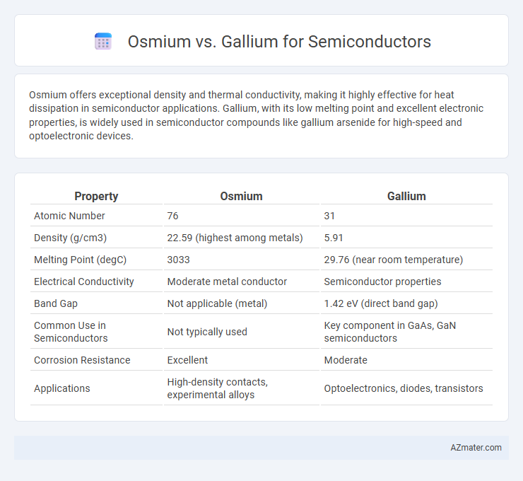
| Property | Osmium | Gallium |
|---|---|---|
| Atomic Number | 76 | 31 |
| Density (g/cm3) | 22.59 (highest among metals) | 5.91 |
| Melting Point (degC) | 3033 | 29.76 (near room temperature) |
| Electrical Conductivity | Moderate metal conductor | Semiconductor properties |
| Band Gap | Not applicable (metal) | 1.42 eV (direct band gap) |
| Common Use in Semiconductors | Not typically used | Key component in GaAs, GaN semiconductors |
| Corrosion Resistance | Excellent | Moderate |
| Applications | High-density contacts, experimental alloys | Optoelectronics, diodes, transistors |
Introduction to Osmium and Gallium
Osmium and gallium are transition metals with unique properties that influence their application in semiconductors. Osmium, known for its density and hardness, offers exceptional stability and conductivity, making it suitable for high-performance electronic components. Gallium exhibits a low melting point and excellent electrical properties, prominently used in the manufacture of gallium arsenide (GaAs) semiconductors, which are essential for high-speed and optoelectronic devices.
Elemental Properties Comparison
Osmium exhibits exceptional thermal and electrical conductivity with a melting point of 3045degC, making it highly stable under extreme conditions ideal for semiconductor applications requiring durability. Gallium has a low melting point of 29.76degC and excellent electron mobility, enabling its widespread use in gallium arsenide (GaAs) semiconductors critical for high-speed electronics. The dense atomic structure and corrosion resistance of osmium contrast with gallium's malleability and reactivity, impacting their suitability in different semiconductor device environments.
Electronic Band Structure Analysis
Osmium exhibits a complex electronic band structure characterized by a high density of states near the Fermi level, contributing to its robust metallic conductivity, making it less suitable for traditional semiconductor applications. Gallium, particularly in the form of gallium arsenide (GaAs), demonstrates a direct band gap with efficient electron mobility and minimal recombination rates, essential for high-performance semiconductor devices. Detailed band structure analysis reveals gallium's superior capacity for electron-hole pair generation and transport, positioning it as a preferred material in optoelectronics and high-frequency semiconductor technology compared to osmium's predominantly metallic behavior.
Role in Modern Semiconductor Devices
Osmium offers exceptional stability and conductivity, making it ideal for high-performance contacts and interconnects in advanced semiconductor devices. Gallium, particularly in the form of gallium arsenide (GaAs) and gallium nitride (GaN), plays a crucial role in high-frequency, optoelectronic, and power semiconductor applications due to its superior electron mobility and wide bandgap properties. The complementary characteristics of osmium's durability and gallium's electronic versatility drive innovations in modern semiconductor technology for faster, more efficient devices.
Electrical Conductivity and Performance
Osmium exhibits higher electrical conductivity compared to gallium, making it more efficient for electron transport in semiconductor applications. Gallium, often used in compounds like gallium arsenide, offers superior semiconductor properties such as direct bandgap and high electron mobility, essential for high-frequency and optoelectronic devices. While osmium provides metallic conductivity, gallium-based semiconductors deliver better overall performance in integrated circuits and photonics due to their tunable electronic properties.
Thermal Stability and Durability
Osmium exhibits exceptional thermal stability and durability, making it highly suitable for high-temperature semiconductor applications where resistance to oxidation and mechanical wear is critical. Gallium, although essential for semiconductor compounds like gallium arsenide, has lower thermal stability and tends to melt near room temperature, limiting its use in extreme thermal environments. The robust atomic structure of osmium provides superior longevity and performance under thermal stress compared to the softer and more reactive gallium.
Manufacturing and Processing Challenges
Osmium's extreme hardness and high melting point pose significant challenges in semiconductor manufacturing, requiring specialized equipment and processes for deposition and etching. In contrast, gallium, with its low melting point and good electrical properties, is easier to process but demands careful handling due to its toxicity and tendency to diffuse into other materials. Both materials necessitate precise control over purity and integration techniques to optimize performance in advanced semiconductor devices.
Environmental and Safety Considerations
Osmium's extreme density and toxicity require stringent handling protocols to prevent environmental contamination and human exposure, making it less favorable for semiconductor applications. Gallium, while less toxic and more environmentally benign, poses challenges due to its melting point near room temperature and potential oxidation, which necessitates careful storage and disposal practices. Both elements demand consideration of lifecycle impacts, but gallium's relative safety and lower environmental risk provide advantages in sustainable semiconductor manufacturing.
Current Applications in the Semiconductor Industry
Osmium and gallium serve distinct roles in the semiconductor industry, with gallium being prominently used in the production of gallium arsenide (GaAs) and gallium nitride (GaN) semiconductors, which are crucial for high-frequency and high-power applications like 5G technology and LED manufacturing. Osmium's application remains limited but is researched for its potential in ultra-durable contacts and thin-film resistors due to its hardness and electrical conductivity. Gallium's widespread adoption in optoelectronics and power devices strongly contrasts with osmium's niche experimental uses in semiconductor components.
Future Prospects: Osmium vs Gallium
Osmium exhibits exceptional electron mobility and thermal stability, making it a promising candidate for high-performance semiconductor applications in extreme environments. Gallium, particularly in the form of gallium arsenide (GaAs), remains dominant in optoelectronics and high-frequency devices due to its established manufacturing infrastructure and superior electron mobility compared to silicon. Future prospects for osmium hinge on overcoming synthesis challenges and cost, while gallium's evolution depends on improved integration with silicon technologies and expanding applications in 5G and beyond.
Infographic: Osmium vs Gallium for Semiconductor