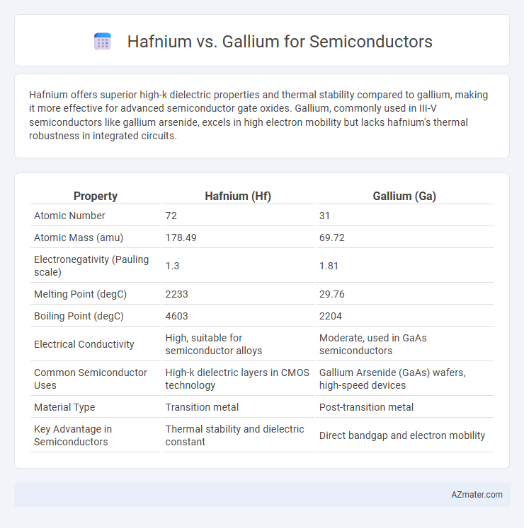
Hafnium offers superior high-k dielectric properties and thermal stability compared to gallium, making it more effective for advanced semiconductor gate oxides. Gallium, commonly used in III-V semiconductors like gallium arsenide, excels in high electron mobility but lacks hafnium's thermal robustness in integrated circuits.
Table of Comparison
| Property | Hafnium (Hf) | Gallium (Ga) |
|---|---|---|
| Atomic Number | 72 | 31 |
| Atomic Mass (amu) | 178.49 | 69.72 |
| Electronegativity (Pauling scale) | 1.3 | 1.81 |
| Melting Point (degC) | 2233 | 29.76 |
| Boiling Point (degC) | 4603 | 2204 |
| Electrical Conductivity | High, suitable for semiconductor alloys | Moderate, used in GaAs semiconductors |
| Common Semiconductor Uses | High-k dielectric layers in CMOS technology | Gallium Arsenide (GaAs) wafers, high-speed devices |
| Material Type | Transition metal | Post-transition metal |
| Key Advantage in Semiconductors | Thermal stability and dielectric constant | Direct bandgap and electron mobility |
Introduction to Hafnium and Gallium in Semiconductors
Hafnium plays a crucial role in semiconductor technology as a high-k dielectric material used to improve transistor gate performance by reducing leakage current and allowing for further device scaling. Gallium is fundamental in semiconductor applications, particularly in gallium arsenide (GaAs) and gallium nitride (GaN) compounds, offering superior electron mobility and wide bandgap properties essential for high-frequency and power devices. Both elements enable advancements in semiconductor efficiency, with hafnium enhancing gate oxides and gallium enabling faster, high-power electronic and optoelectronic components.
Atomic Structure and Chemical Properties
Hafnium (Hf) exhibits an atomic number of 72 with a dense d-block electron configuration [Xe] 4f14 5d2 6s2, contributing to its high melting point and excellent thermal stability, essential for semiconductor applications requiring heat resistance. Gallium (Ga), atomic number 31, has an electron configuration of [Ar] 3d10 4s2 4p1, characterized by a lower melting point and unique liquid phase near room temperature, allowing for versatile uses in semiconductors like gallium arsenide (GaAs) with superior electron mobility. The chemical inertness and corrosion resistance of hafnium enhance its durability in semiconductor devices, while gallium's ability to form stable covalent bonds and compound semiconductors underpins its pivotal role in high-speed and optoelectronic applications.
Material Abundance and Sourcing
Hafnium and gallium are critical elements in semiconductor manufacturing, with gallium being more abundant and commercially available due to its primary extraction from bauxite and zinc ores. Hafnium, a rare transition metal primarily sourced as a byproduct of zirconium refining, faces limited global reserves, influencing its higher cost and constrained supply chain. The relative abundance and sourcing complexity of gallium provide more stable material availability for large-scale semiconductor production compared to the scarcity-driven limitations of hafnium.
Integration in Modern Semiconductor Fabrication
Hafnium and Gallium play crucial roles in modern semiconductor fabrication, with Hafnium primarily used in high-k dielectric materials to enhance transistor gate performance by reducing leakage currents at nanoscale dimensions. Gallium, especially in the form of Gallium Arsenide (GaAs) and Gallium Nitride (GaN), is integral to high-speed and high-frequency applications, offering superior electron mobility compared to silicon. The integration challenges differ as Hafnium oxide layers seamlessly integrate into existing silicon processes, whereas Gallium-based compounds require specialized substrates and epitaxial growth techniques for optimal device performance.
Electrical Conductivity and Performance Metrics
Hafnium exhibits lower electrical conductivity compared to gallium but offers exceptional thermal stability and high dielectric constant, making it ideal for advanced semiconductor gate dielectrics. Gallium, especially in compounds like gallium arsenide, provides superior electron mobility and higher electrical conductivity, enhancing high-frequency and optoelectronic device performance. Performance metrics highlight gallium's advantage in speed and efficiency, while hafnium's strength lies in reliability and scaling for next-generation transistor technologies.
Thermal Stability and Reliability
Hafnium exhibits superior thermal stability compared to gallium, making it more suitable for high-temperature semiconductor applications where material integrity is critical. Its high melting point and excellent resistance to oxidation enhance device reliability under thermal stress conditions. Gallium, while useful in specific compound semiconductors like GaAs, typically demonstrates lower thermal stability and may degrade faster in harsh operating environments.
Cost Analysis and Economic Viability
Hafnium, a high-k dielectric material, offers superior performance in semiconductor manufacturing but comes at a significantly higher cost due to limited global supply and complex extraction processes. In contrast, gallium, essential for III-V semiconductors like gallium arsenide, provides a more cost-effective option with broader availability and established recycling methods, making it economically viable for large-scale production. The cost analysis favors gallium for applications requiring balanced performance and affordability, while hafnium remains reserved for specialized, high-performance components where expense is justified.
Environmental Impact and Sustainability
Hafnium and gallium both play crucial roles in semiconductor manufacturing, but differ significantly in environmental impact and sustainability. Hafnium is more abundant in nature and exhibits better recyclability, reducing the strain on mining resources and lowering ecological footprints. In contrast, gallium extraction often involves energy-intensive processes with potential hazardous waste, raising concerns about long-term environmental sustainability in semiconductor production.
Industry Applications and Current Use Cases
Hafnium's high dielectric constant makes it essential in advanced semiconductor manufacturing, particularly for gate insulators in high-performance transistors used in microprocessors and memory devices. Gallium, primarily in the form of gallium arsenide (GaAs) and gallium nitride (GaN), dominates in high-frequency and optoelectronic applications, including RF amplifiers, LED lighting, and power electronics. The complementary roles of hafnium and gallium compounds enable innovation across industries such as telecommunications, consumer electronics, and renewable energy systems.
Future Prospects in Semiconductor Technology
Hafnium shows promising potential in advanced semiconductor gate dielectrics due to its high dielectric constant and thermal stability, enabling further scaling of transistor technology beyond silicon dioxide limits. Gallium, particularly in the form of gallium nitride (GaN), advances high-power and high-frequency semiconductor devices, offering superior electron mobility and thermal conductivity compared to silicon, which is crucial for 5G and beyond communication technologies. The future semiconductor landscape will likely leverage hafnium's integration for miniaturization alongside gallium's applications in power-efficient, high-performance devices, driving innovation in both logic and RF electronics.
Infographic: Hafnium vs Gallium for Semiconductor