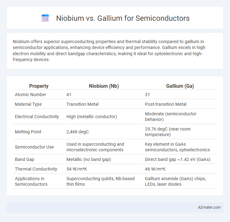
Niobium offers superior superconducting properties and thermal stability compared to gallium in semiconductor applications, enhancing device efficiency and performance. Gallium excels in high electron mobility and direct bandgap characteristics, making it ideal for optoelectronic and high-frequency devices.
Table of Comparison
| Property | Niobium (Nb) | Gallium (Ga) |
|---|---|---|
| Atomic Number | 41 | 31 |
| Material Type | Transition Metal | Post-transition Metal |
| Electrical Conductivity | High (metallic conductor) | Moderate (semiconductor behavior) |
| Melting Point | 2,468 degC | 29.76 degC (near room temperature) |
| Semiconductor Use | Used in superconducting and microelectronic components | Key element in GaAs semiconductors, optoelectronics |
| Band Gap | Metallic (no band gap) | Direct band gap ~1.42 eV (GaAs) |
| Thermal Conductivity | 54 W/m*K | 46 W/m*K |
| Applications in Semiconductors | Superconducting qubits, Nb-based thin films | Gallium arsenide (GaAs) chips, LEDs, laser diodes |
Introduction to Niobium and Gallium in Semiconductors
Niobium and Gallium are critical elements in semiconductor technology, each offering unique electrical properties essential for device performance. Niobium is valued for its superconducting capabilities and high melting point, making it suitable for high-frequency and quantum computing applications. Gallium, particularly in the form of gallium arsenide (GaAs), is widely used for its superior electron mobility and direct bandgap, enabling efficient optoelectronic devices and high-speed integrated circuits.
Atomic Structure and Material Properties
Niobium, with atomic number 41 and electron configuration [Kr] 4d4 5s1, exhibits a body-centered cubic crystal structure, offering high melting points (2477degC) and excellent superconducting properties, making it suitable for specialized semiconductor applications requiring stability under extreme conditions. Gallium, atomic number 31 and electron configuration [Ar] 3d10 4s2 4p1, crystallizes in an orthorhombic structure with a low melting point (29.76degC) and unique semiconducting characteristics, widely used in gallium arsenide (GaAs) compounds for high-speed and optoelectronic devices. The distinct atomic structures and melting points of niobium and gallium directly influence their electrical conductivity, thermal stability, and integration potential in advanced semiconductor technologies.
Electrical Conductivity Comparison
Niobium exhibits moderate electrical conductivity with values typically around 6.7 x 10^6 S/m, making it suitable for certain semiconductor applications requiring stability at high temperatures. Gallium, particularly in its liquid phase or as gallium-based compounds like gallium arsenide (GaAs), offers significantly higher electrical conductivity and electron mobility, crucial for high-speed electronic devices. The superior conductivity and direct bandgap of gallium compounds provide distinct advantages over niobium in semiconductor performance, particularly in optoelectronics and high-frequency circuits.
Thermal Stability and Heat Resistance
Niobium exhibits superior thermal stability and heat resistance compared to gallium, making it ideal for high-temperature semiconductor applications. Niobium-based compounds maintain structural integrity and electrical performance at temperatures exceeding 1500degC, whereas gallium's heat resistance is typically limited below 900degC due to its low melting point. This thermal advantage positions niobium as a preferred material for power electronics and devices operating in extreme thermal environments.
Applications in Modern Semiconductor Devices
Niobium exhibits excellent superconducting properties, making it ideal for quantum computing components and high-frequency superconducting circuits in modern semiconductor devices. Gallium, primarily used in gallium arsenide (GaAs) and gallium nitride (GaN) semiconductors, enables high-speed, high-efficiency electronics and optoelectronic applications like LEDs, laser diodes, and RF amplifiers. The choice between niobium and gallium depends on the specific device requirements, with niobium favoring superconducting and cryogenic applications, while gallium is preferred for high-power and high-frequency semiconductor technologies.
Bandgap Energy Differences
Niobium exhibits a bandgap energy typically in the range of 0.1 to 0.2 eV when used in semiconductor applications, indicating its suitability for infrared detection and low-energy electronic devices. Gallium compounds, especially gallium arsenide (GaAs), have a wider direct bandgap of approximately 1.42 eV, enabling high-speed and optoelectronic applications such as LEDs and solar cells. The significant bandgap energy difference between niobium-based and gallium-based semiconductors influences their electron mobility, absorption spectra, and device performance parameters.
Fabrication and Material Sourcing
Niobium offers superior thermal stability and is extensively used in superconducting semiconductor fabrication, providing enhanced performance for quantum devices. Gallium, primarily sourced from bauxite refining and zinc mining by-products, is crucial for producing gallium arsenide (GaAs) semiconductors, known for high electron mobility and optoelectronic applications. Material sourcing for niobium is geographically concentrated in Brazil and Canada, whereas gallium supply relies on more dispersed and less abundant sources, influencing cost and availability in semiconductor manufacturing.
Cost and Economic Considerations
Niobium presents a higher upfront cost compared to gallium, largely due to its rarer availability and complex extraction processes, which can elevate semiconductor production expenses. Gallium remains more economically viable, benefiting from established supply chains and higher market demand, driving down per-unit costs in semiconductor manufacturing. Evaluating long-term investment, gallium's cost efficiency supports scalability, whereas niobium's premium pricing may restrict its use to niche applications where superior performance justifies the expense.
Environmental Impact and Sustainability
Niobium's widespread use in semiconductor applications leverages its rarity and recyclability, resulting in a lower environmental footprint compared to gallium, which faces higher extraction energy demands and potential toxicity concerns. Gallium's sourcing from bauxite and zinc ores involves intensive mining practices, leading to significant habitat disruption and waste generation, whereas niobium often benefits from deposits with lower ecological disturbance. Sustainable semiconductor manufacturing increasingly favors niobium due to its long-term availability and reduced reliance on environmentally damaging refining processes.
Future Prospects in Semiconductor Technology
Niobium's high melting point, excellent superconducting properties, and compatibility with silicon make it a promising candidate for next-generation quantum computing and high-speed electronics. Gallium, particularly in the form of gallium arsenide (GaAs) and gallium nitride (GaN), dominates current semiconductor technology due to superior electron mobility and efficiency in high-frequency and optoelectronic applications. Future prospects suggest niobium-based materials could complement gallium compounds by enabling more robust superconducting devices and energy-efficient components in integrated circuits.
Infographic: Niobium vs Gallium for Semiconductor