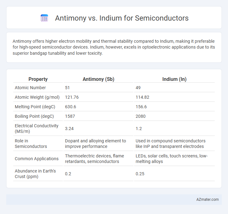
Antimony offers higher electron mobility and thermal stability compared to Indium, making it preferable for high-speed semiconductor devices. Indium, however, excels in optoelectronic applications due to its superior bandgap tunability and lower toxicity.
Table of Comparison
| Property | Antimony (Sb) | Indium (In) |
|---|---|---|
| Atomic Number | 51 | 49 |
| Atomic Weight (g/mol) | 121.76 | 114.82 |
| Melting Point (degC) | 630.6 | 156.6 |
| Boiling Point (degC) | 1587 | 2080 |
| Electrical Conductivity (MS/m) | 3.24 | 1.2 |
| Role in Semiconductors | Dopant and alloying element to improve performance | Used in compound semiconductors like InP and transparent electrodes |
| Common Applications | Thermoelectric devices, flame retardants, semiconductors | LEDs, solar cells, touch screens, low-melting alloys |
| Abundance in Earth's Crust (ppm) | 0.2 | 0.25 |
Introduction to Antimony and Indium in Semiconductors
Antimony and indium are critical elements in semiconductor technology, each offering unique electronic properties for device fabrication. Antimony is primarily used in the formation of III-V compound semiconductors such as indium antimonide (InSb) and gallium antimonide (GaSb), which exhibit high electron mobility and direct bandgaps suitable for infrared detectors and high-speed electronics. Indium plays a pivotal role in indium phosphide (InP) and indium gallium arsenide (InGaAs) semiconductors, valued for their excellent electron transport characteristics and efficiency in optoelectronic applications like lasers and photodetectors.
Elemental Properties: Antimony vs Indium
Antimony exhibits a higher atomic number (51) and greater density (6.697 g/cm3) compared to Indium's atomic number of 49 and density of 7.31 g/cm3, influencing their electrical and thermal conductivity in semiconductor applications. Antimony's electron configuration ([Kr] 4d10 5s2 5p3) lends itself to n-type doping, while Indium ([Kr] 4d10 5s2 5p1) often serves as a p-type dopant or in transparent conductive oxides due to its unique valence electron structure. The melting points, 630.63degC for Antimony and 156.6degC for Indium, further affect their suitability in high-temperature semiconductor manufacturing processes.
Electronic Characteristics and Band Gap Comparison
Antimony exhibits a band gap of approximately 1.22 eV, making it suitable for infrared detectors and thermoelectric applications, while indium's band gap varies depending on its compound form, such as indium arsenide (~0.36 eV) and indium phosphide (~1.35 eV), which are favored for high-speed and optoelectronic devices. Electron mobility in indium-based semiconductors typically surpasses that of antimony, enabling faster electronic switching and improved device performance. The choice between antimony and indium depends on the specific semiconductor application requirements, where band gap and electron mobility critically influence device efficiency and operating wavelength.
Role in Compound Semiconductors
Antimony (Sb) is commonly used as a group V element in III-V compound semiconductors such as InSb and GaSb, providing excellent electron mobility and narrow bandgap properties essential for high-speed and infrared applications. Indium (In), a group III element, forms crucial components in compounds like InP, InAs, and InGaAs, offering superior lattice matching and high electron velocity crucial for optoelectronic devices and high-frequency transistors. The complementary roles of Sb and In enable the engineering of materials with tailored bandgaps, electron transport properties, and lattice constants for advanced semiconductor devices.
Application Differences in Electronics
Antimony is primarily used as a dopant in semiconductor devices to enhance electrical conductivity, particularly in silicon-based components like diodes and infrared detectors. Indium, on the other hand, plays a crucial role in the formation of indium phosphide (InP) and indium tin oxide (ITO), which are essential for high-speed transistors, solar cells, and transparent conductive coatings in displays. The distinct electronic and optical properties of antimony and indium drive their application differences, with antimony focusing on doping efficiency and indium enabling advanced optoelectronic and display technologies.
Material Availability and Sourcing
Antimony is more abundant in the Earth's crust and is primarily sourced from China, Russia, and Bolivia, making it relatively accessible for semiconductor manufacturing. Indium, with a rarer concentration primarily obtained as a byproduct of zinc mining in countries like China, South Korea, and Canada, faces tighter supply constraints and higher market volatility. The limited global reserves and increasing demand for indium challenge its sourcing compared to the more readily available antimony, impacting long-term material sustainability in semiconductor applications.
Performance in Advanced Device Fabrication
Antimony offers superior electron mobility compared to indium, making it highly effective for high-speed semiconductor applications and advanced device fabrication. Indium, particularly in indium gallium arsenide (InGaAs) compounds, excels in infrared detection and high-frequency transistors due to its favorable bandgap and carrier velocity. The choice between antimony and indium impacts device performance metrics such as switching speed, thermal stability, and integration with silicon technology in advanced semiconductor manufacturing.
Environmental Impact and Toxicity Concerns
Antimony and indium, both critical in semiconductor manufacturing, pose distinct environmental and toxicity challenges. Antimony compounds are highly toxic, linked to respiratory and skin issues, with persistent environmental contamination potential during mining and processing. Indium exhibits lower acute toxicity but presents risks from indium-containing dust and waste, necessitating stringent controls to mitigate environmental accumulation and worker exposure.
Cost Efficiency and Market Trends
Antimony offers superior cost efficiency compared to indium due to its greater abundance and lower extraction costs, making it a favorable choice in semiconductor manufacturing. Market trends indicate increasing demand for indium in high-performance applications despite its higher price, driven by its unique electrical properties and use in thin-film transistors and transparent conductive oxides. Semiconductor industries are increasingly balancing antimony's affordability with indium's performance advantages to optimize production costs and device efficiency.
Future Prospects: Antimony and Indium in Next-Generation Semiconductors
Antimony and Indium are critical materials for next-generation semiconductors due to their unique electronic properties and compatibility with emerging device architectures. Antimony's role in high-speed transistors and infrared detectors positions it as a key element for advanced optoelectronic applications, while Indium's contributions in indium gallium arsenide (InGaAs) and indium phosphide (InP) compounds underpin its significance in high-frequency and photonic devices. Ongoing research in integrating these elements aims to enhance performance efficiencies, enabling breakthroughs in quantum computing, 5G technologies, and flexible electronics.
Infographic: Antimony vs Indium for Semiconductor