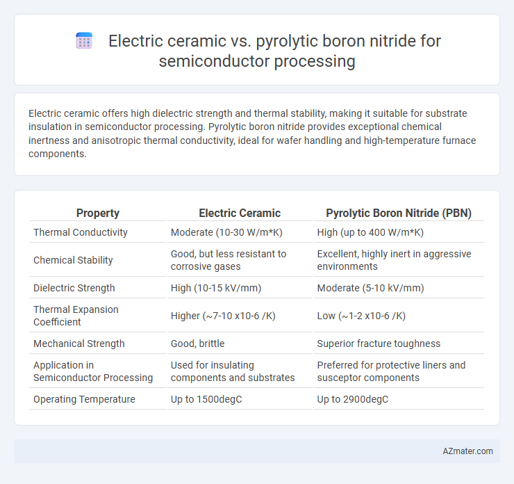
Electric ceramic offers high dielectric strength and thermal stability, making it suitable for substrate insulation in semiconductor processing. Pyrolytic boron nitride provides exceptional chemical inertness and anisotropic thermal conductivity, ideal for wafer handling and high-temperature furnace components.
Table of Comparison
| Property | Electric Ceramic | Pyrolytic Boron Nitride (PBN) |
|---|---|---|
| Thermal Conductivity | Moderate (10-30 W/m*K) | High (up to 400 W/m*K) |
| Chemical Stability | Good, but less resistant to corrosive gases | Excellent, highly inert in aggressive environments |
| Dielectric Strength | High (10-15 kV/mm) | Moderate (5-10 kV/mm) |
| Thermal Expansion Coefficient | Higher (~7-10 x10-6 /K) | Low (~1-2 x10⁻⁶ /K) |
| Mechanical Strength | Good, brittle | Superior fracture toughness |
| Application in Semiconductor Processing | Used for insulating components and substrates | Preferred for protective liners and susceptor components |
| Operating Temperature | Up to 1500degC | Up to 2900degC |
Introduction to Wafer Carrier Materials in Semiconductor Processing
Electric ceramic and pyrolytic boron nitride (PBN) are critical materials used in wafer carriers for semiconductor processing, offering distinct thermal and chemical properties essential for high-precision environments. Electric ceramics provide excellent electrical insulation and high thermal stability, making them suitable for thermally demanding processes, while PBN offers superior chemical inertness and exceptional thermal shock resistance, minimizing contamination risks during wafer handling. Choosing the appropriate wafer carrier material directly impacts yield and device performance by ensuring optimal thermal management and preventing particle generation in cleanroom semiconductor fabrication.
Overview of Electric Ceramic: Composition and Properties
Electric ceramic in semiconductor processing is typically composed of materials such as aluminum oxide (Al2O3), aluminum nitride (AlN), and silicon nitride (Si3N4), known for their high electrical insulation, thermal stability, and mechanical strength. These ceramics offer excellent dielectric properties, enabling efficient isolation of electrical components and resistance to high temperatures and chemical corrosion. Their versatility and cost-effectiveness make electric ceramics a preferred choice for packaging and insulating semiconductor devices compared to pyrolytic boron nitride, which is valued for its superior thermal conductivity and chemical inertness.
Pyrolytic Boron Nitride: Structure and Material Advantages
Pyrolytic boron nitride (PBN) features a hexagonal layered structure with exceptional thermal stability, chemical inertness, and low dielectric constant, making it ideal for semiconductor processing applications. Its high purity and uniformity provide superior resistance to contamination and corrosion compared to traditional electric ceramics, enhancing wafer yield and device performance. The anisotropic thermal conductivity of PBN ensures efficient heat dissipation, critical for high-temperature semiconductor manufacturing environments.
Thermal Stability Comparison Under High-Temperature Processing
Electric ceramic materials exhibit moderate thermal stability with operational limits generally up to 1,200degC, making them suitable for many semiconductor processes but potentially vulnerable to degradation under extended high-temperature exposure. Pyrolytic boron nitride (PBN) demonstrates superior thermal stability, maintaining structural integrity and chemical inertness at temperatures exceeding 2,700degC, which ensures reliability during aggressive high-temperature semiconductor manufacturing steps such as epitaxial growth or diffusion. The exceptional thermal conductivity and resistance to thermal shock of PBN provide enhanced performance and longer service life compared to standard electric ceramics in thermal-intensive environments.
Chemical Resistance to Plasma and Reactive Gases
Electric ceramic materials exhibit strong chemical resistance to plasma and reactive gases, making them suitable for semiconductor processing environments with moderate reactivity levels. Pyrolytic boron nitride (PBN) outperforms electric ceramics due to its exceptional stability against aggressive plasma chemistries and reactive gases such as fluorine and chlorine-based compounds. The superior inertness and low reactivity of PBN reduce contamination risks and extend component lifetimes in harsh semiconductor manufacturing processes.
Mechanical Strength and Longevity in Cleanroom Environments
Electric ceramic materials exhibit higher mechanical strength compared to pyrolytic boron nitride, making them more resistant to wear and deformation in semiconductor processing equipment. Pyrolytic boron nitride offers superior chemical stability and thermal shock resistance, enhancing its longevity in cleanroom environments despite having lower mechanical strength. Choosing between electric ceramic and pyrolytic boron nitride depends on the specific demands of mechanical durability versus chemical inertness and thermal resilience in semiconductor manufacturing.
Impact on Semiconductor Yield and Defect Reduction
Electric ceramic materials exhibit high dielectric strength and chemical resistance, contributing to improved semiconductor yield by minimizing contamination and electrical failures during processing. Pyrolytic boron nitride (PBN) offers exceptional thermal stability and high purity, significantly reducing particle generation and defects that directly impact device performance. The superior inertness and uniformity of PBN substrates lead to fewer wafer defects and higher overall yield in advanced semiconductor manufacturing environments.
Compatibility with Etching and Deposition Processes
Electric ceramic materials exhibit high chemical resistance and thermal stability, making them compatible with most semiconductor etching and deposition environments, particularly in plasma and reactive ion etching setups. Pyrolytic boron nitride offers superior thermal conductivity and chemical inertness, enabling it to withstand aggressive fluorine-based etchants and high-temperature chemical vapor deposition without degradation. Pyrolytic boron nitride's anisotropic structure enhances process uniformity and reduces contamination risks, providing a performance edge in advanced semiconductor fabrication over conventional electric ceramics.
Cost-Effectiveness and Supply Chain Considerations
Electric ceramic materials offer a cost-effective solution for semiconductor processing due to lower raw material and manufacturing expenses compared to pyrolytic boron nitride (PBN), which involves complex synthesis and higher purity requirements. Supply chain stability favors electric ceramics as they are widely produced and readily available, whereas PBN's specialized production and limited suppliers can lead to longer lead times and price volatility. Semiconductor manufacturers must weigh these factors against performance needs, balancing cost-efficiency with material properties critical for high-temperature and chemical resistance environments.
Future Trends in Wafer Carrier Material Innovation
Electric ceramic wafer carriers offer high electrical insulation and thermal stability essential for semiconductor processing, but pyrolytic boron nitride (PBN) stands out with superior chemical inertness and exceptional thermal conductivity, enabling better contamination control and process uniformity. Future trends in wafer carrier materials emphasize enhancing thermal management and contamination resistance, driving innovation in composite structures that combine the robustness of electric ceramics with the surface properties of PBN. Integration of advanced coatings and nano-engineered interfaces is expected to extend carrier lifespan and support the increasing demands of next-generation semiconductor devices.
Infographic: Electric ceramic vs Pyrolytic boron nitride for Semiconductor processing