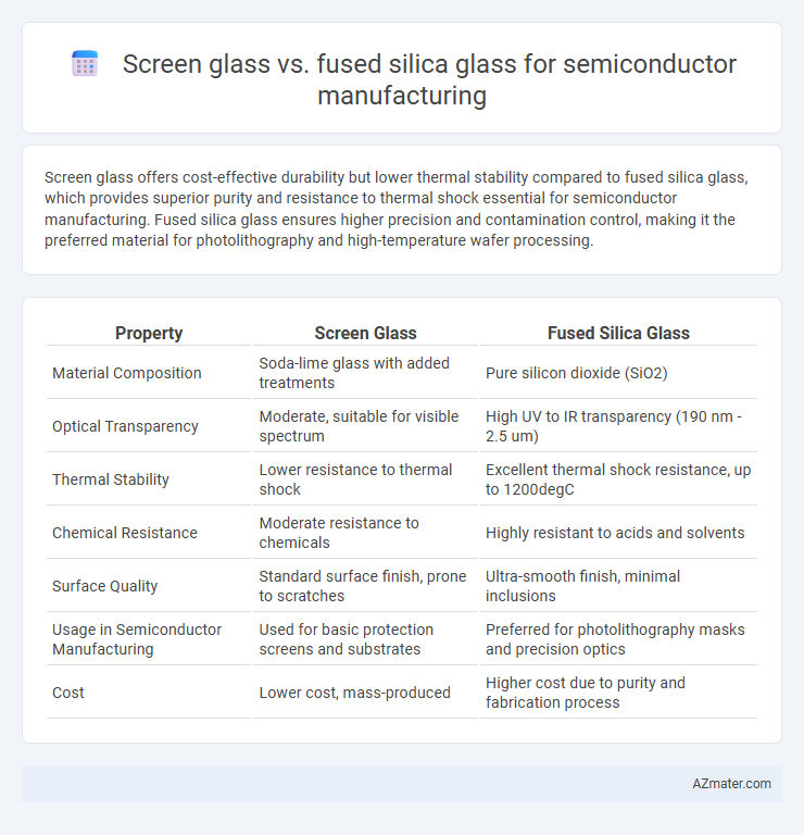
Screen glass offers cost-effective durability but lower thermal stability compared to fused silica glass, which provides superior purity and resistance to thermal shock essential for semiconductor manufacturing. Fused silica glass ensures higher precision and contamination control, making it the preferred material for photolithography and high-temperature wafer processing.
Table of Comparison
| Property | Screen Glass | Fused Silica Glass |
|---|---|---|
| Material Composition | Soda-lime glass with added treatments | Pure silicon dioxide (SiO2) |
| Optical Transparency | Moderate, suitable for visible spectrum | High UV to IR transparency (190 nm - 2.5 um) |
| Thermal Stability | Lower resistance to thermal shock | Excellent thermal shock resistance, up to 1200degC |
| Chemical Resistance | Moderate resistance to chemicals | Highly resistant to acids and solvents |
| Surface Quality | Standard surface finish, prone to scratches | Ultra-smooth finish, minimal inclusions |
| Usage in Semiconductor Manufacturing | Used for basic protection screens and substrates | Preferred for photolithography masks and precision optics |
| Cost | Lower cost, mass-produced | Higher cost due to purity and fabrication process |
Introduction to Glass Types in Semiconductor Manufacturing
Screen glass and fused silica glass are critical materials in semiconductor manufacturing, each offering distinct physical and chemical properties suited for different applications. Screen glass typically refers to aluminosilicate glass with higher mechanical strength and thermal durability, ideal for protective screens in semiconductor equipment. Fused silica glass, composed of high-purity silicon dioxide, provides exceptional thermal stability, chemical resistance, and optical clarity, making it essential for photolithography masks and precision optical components in semiconductor fabrication.
What is Screen Glass?
Screen glass, used in semiconductor manufacturing, is a type of borosilicate or aluminosilicate glass designed for durability and chemical resistance during photolithography processes. It serves as a mask or substrate for patterning circuits, maintaining dimensional stability under UV exposure and thermal cycling. Compared to fused silica glass, screen glass offers cost-effective production with adequate optical clarity, though it has higher thermal expansion and lower purity levels.
What is Fused Silica Glass?
Fused silica glass is a high-purity, non-crystalline silicon dioxide material renowned for its exceptional thermal stability, low thermal expansion, and excellent optical transparency in ultraviolet to infrared wavelengths. In semiconductor manufacturing, fused silica glass offers superior resistance to extreme processing temperatures and chemical corrosion compared to conventional screen glass, making it ideal for photomask substrates and precision lithography applications. Its ultra-low impurity levels and homogeneity ensure minimal optical distortions and enhanced durability during high-precision semiconductor fabrication processes.
Key Material Properties: Screen Glass vs Fused Silica
Screen glass offers moderate thermal stability and mechanical strength, making it suitable for general semiconductor display applications but less ideal for high-precision manufacturing. Fused silica glass excels with exceptional thermal resistance, low thermal expansion coefficient (approximately 0.5 x 10^-6 /degC), and superior optical transparency, critical for photolithography and precision semiconductor processes. The ultra-low impurity content and high chemical durability of fused silica ensure enhanced photomask accuracy and longer lifespan in semiconductor fabrication environments.
Thermal Stability and Expansion Characteristics
Screen glass exhibits moderate thermal stability with a higher coefficient of thermal expansion (CTE), making it less ideal for precision semiconductor manufacturing where temperature fluctuations are frequent. Fused silica glass offers superior thermal stability and an ultra-low CTE close to 0.5 x 10^-6 /degC, ensuring minimal dimensional changes during high-temperature processes. This low expansion characteristic of fused silica is critical for maintaining tight tolerances and preventing stress-induced defects in semiconductor fabrication.
Chemical Resistance and Purity Levels
Fused silica glass exhibits superior chemical resistance and higher purity levels compared to screen glass, making it ideal for semiconductor manufacturing processes that require exposure to aggressive chemicals and contamination-sensitive environments. The ultra-high purity of fused silica minimizes ionic and metallic impurities, thereby preventing defects and ensuring optimal performance in photolithography and wafer processing. In contrast, screen glass, while more economical, typically contains higher levels of impurities and exhibits lower chemical durability, limiting its suitability for precision semiconductor applications.
Optical Clarity and Transmission Differences
Screen glass typically exhibits lower optical clarity and reduced light transmission compared to fused silica glass, which is renowned for its exceptional transparency across a broad spectrum, including UV and IR wavelengths. Fused silica glass features minimal internal defects and a highly uniform molecular structure, resulting in superior optical performance critical for precise photolithography in semiconductor manufacturing. The higher purity and lower scattering properties of fused silica lead to enhanced accuracy and efficiency in semiconductor fabrication processes requiring high-precision optical components.
Cost Comparison in Large-Scale Manufacturing
Screen glass offers a lower initial cost compared to fused silica glass, making it attractive for large-scale semiconductor manufacturing where budget constraints are critical. Fused silica glass, despite its higher price, provides superior thermal stability and chemical resistance, reducing downtime and long-term operational costs. Overall, the cost comparison depends on balancing upfront expenses with durability and performance requirements in high-volume production environments.
Application Suitability: When to Use Each Type
Screen glass offers cost-effective protection and is suitable for general semiconductor manufacturing processes where high thermal resistance is not critical. Fused silica glass provides superior thermal stability, chemical resistance, and optical clarity, making it ideal for high-temperature photolithography and advanced chip fabrication. Use fused silica glass in precision applications requiring minimal thermal expansion and high purity, while screen glass fits non-critical areas with moderate environmental demands.
Future Advances in Semiconductor Glass Materials
Fused silica glass, renowned for its superior thermal stability and low thermal expansion, is increasingly preferred over traditional screen glass in semiconductor manufacturing due to its ability to withstand extreme processing conditions. Future advances focus on enhancing the purity and homogeneity of fused silica to reduce defects and improve lithographic precision at sub-5nm node technologies. Innovations in doped fused silica and hybrid glass composites aim to optimize optical transparency and mechanical strength, addressing the evolving demands of next-generation semiconductor fabrication.
Infographic: Screen glass vs Fused silica glass for Semiconductor manufacturing